
Machine software for 134 wafer inspection systems taken over
EPSIA maintains and develops the control software of 134 wafer inspection systems in series production at a semiconductor manufacturer in Asia. After taking over the existing machine software, EPSIA analysed recurring contacting errors, proved their technical cause and developed a new alignment method. It reduces the alignment time for an 8-inch wafer from 7:44 to 1:16 minutes.
- −84 %alignment time per wafer, 1:16 instead of 7:44 minutes
- 4–5 µmpositioning accuracy (3σ) with up to 130,000 dies
- 134systems in series production
- 5–10 µmposition error proven as the cause of the contacting errors
The case study follows the project in seven steps: takeover, analysis, root cause, proof of feasibility, solution, integration and result.
1 Takeover: Continuing series production without the original manufacturer
The wafer inspection systems maintained by EPSIA optically align chips for SAW filters on an 8-inch wafer and contact every single die for electrical testing. Depending on the product, a wafer carries between 17,709 and 150,198 dies; a typical pitch is 0.43 × 0.43 mm.
When the original manufacturer could no longer maintain the machine software, EPSIA took over the source code and software maintenance. The first goal was to be able to develop the existing software reliably without interrupting ongoing production.
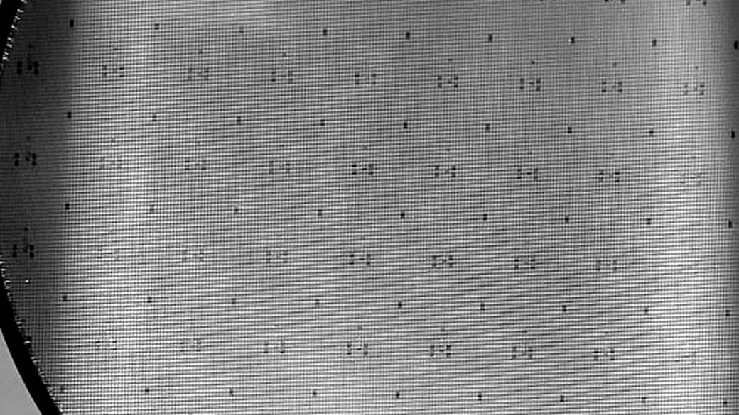
The C++ software has grown since 2015, controls three machine variants and contains changes by more than ten developers. It integrates servo axes via CAN, inputs and outputs via EtherCAT, and industrial image processing with MVTec HALCON.
EPSIA restored the development and build environment, analysed the architecture and interfaces and documented the existing system. Series production continued throughout the takeover; since then, EPSIA has implemented new requirements and software changes.
Scope of the software taken over
- Lines of code
- 333,237 in 2,744 files
- Classes
- 1,913
- Changes
- 8,623 since 2015
- Variants
- 3 machine types
- Axes
- 6 servo axes with Elmo drives on the CAN bus
- I/O signals
- 81 to 92 via Beckhoff terminals on EtherCAT
- Interfaces
- MVTec HALCON, measurement computer, wafer robot and MySQL
- Toolchain
- Qt 4.8 and 5.9, MinGW, qmake, Jenkins
2 Analysis: Making position errors visible for every die
The wafer inspection systems must contact every die with probes to within a few micrometres. Positioning deviations can lead to faulty contacts and thus to quality losses in testing.
To investigate intermittent deviations systematically, EPSIA developed its own analysis tool in 2023 and 2024. It reconstructs the position deviation of every single die on a wafer from proprietary, rotating log files.
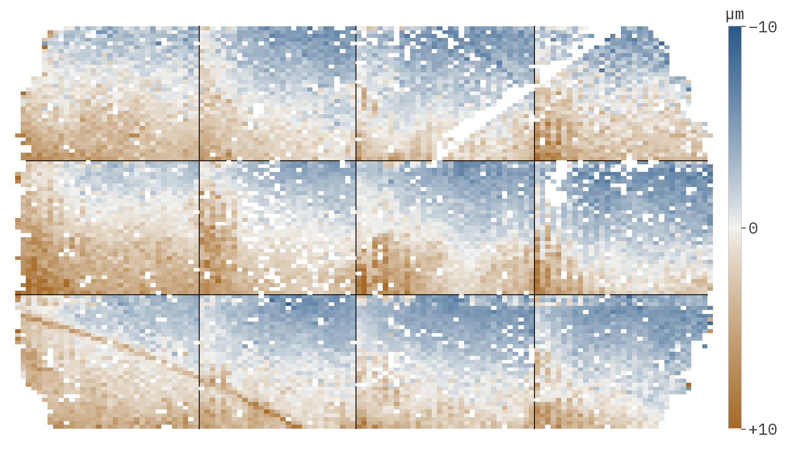
For one product examined, this means evaluating 17,709 dies of 1.03 × 0.73 mm each. A wafer map shows the deviation of each die on a scale from −10 to +10 µm. In addition, a statistical evaluation summarises the positioning accuracy of each wafer as a 3σ ellipse.
3 Root cause: Optical distortion at the edge of the camera's field of view
The original alignment captured the wafer sector by sector with the camera and derived the position of the individual dies from these images.
The analysis developed by EPSIA revealed a systematic error pattern at the edges of these sectors. The cause was optical distortion at the edge of the camera's field of view. There, die positions were determined with an offset of 5 to 10 µm – a deviation that could exceed the permitted positioning tolerance.
In addition, the complete optical pre-measurement took more than six minutes for every wafer.
4 Feasibility: New alignment first tested in simulation
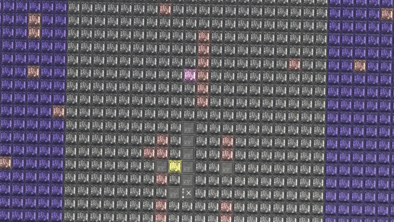
Before EPSIA changed the software of a production system, the new alignment method was tested in a 3D simulation.
A virtual wafer is deliberately shifted in X and Y and rotated by a defined angle. The software then detects reference marks and calculates the shift and rotation of the wafer on its own.
A proof of concept on a real system confirmed the method in September 2024.
5 Solution: M.A.P. calculates die positions from reference marks
With M.A.P. – Map Alignment and Positioning – EPSIA developed a new alignment method. Instead of photographing the entire wafer sector by sector before testing, the camera captures only selected reference marks. The positions of all other dies are then calculated from the wafer map.
The method works in several steps:
- For pairs of reference marks, the software compares the target vectors from the wafer map with the measured actual vectors and derives the rotation angle and shift.
- The results from several reference marks are evaluated together.
- The scaling of the wafer along the axes is determined from reference marks that lie far apart.
- The wafer table corrects the rotation until the remaining angle is below 0.01°.
- The position of each die is calculated from map position, scaling, rotation and shift. The correction matrix of the table calibration is also applied.
- Plausibility checks detect special cases. If M.A.P. cannot determine a reliable alignment, the system falls back to the previous method.
6 Integration: Introduction into running series production
EPSIA integrated M.A.P. into the existing machine software as a fixed-price project. EPSIA had no production system of its own available for development.
The software was first tested on a reference system at the machine builder in Berlin and then verified remotely on systems in the customer's series production in Asia. M.A.P. has been in productive use since summer 2025 and now runs on all 134 systems.
In 2026, further functions based on the new position determination followed, including an imprint check and multi-site production, in which up to four dies are contacted simultaneously.
EPSIA also analyses faults from ongoing production remotely. These include, for example, faults in setup wizards and machine sequences.
7 Result: 84 % shorter alignment time with 4 to 5 µm positioning accuracy
The new M.A.P. alignment reduces the time needed to align an 8-inch wafer from 7:44 to 1:16 minutes. That is a reduction of 84 %. The share for the actual pre-measurement falls from 6:12 minutes to 16 seconds.
Measurements in series production show a positioning accuracy of 4.2 × 2.6 µm (3σ) with around 70,000 dies and 5.1 × 1.6 µm (3σ) with around 130,000 dies per wafer.
The measured times also allow an estimate of the potential capacity gain. With a test time of around two hours per wafer and twelve wafers per day, this works out at roughly 78 minutes of additional test time per system per day. That is just over 5 % more usable test time.
Extrapolated across 134 systems, the alignment time saved corresponds to around 63,000 additional test machine hours per year. That equals the annual test time of roughly seven additional systems. These figures are an extrapolation from the measured alignment times and assumed production operation, not a separately measured increase in output.
After the original manufacturer ended its support, series production on 134 systems continued with the software that EPSIA took over and developed further.
What does this project stand for?
The project shows how EPSIA takes over existing machine software and step by step makes it technically manageable again: taking over source code and build environment, understanding a complex existing system, tracing hard-to-reproduce faults to a specific cause using measurement data, simulating a new solution first and then integrating it into a running production environment.
The takeover was therefore not limited to maintaining an existing software version. Building on the system it had taken over, EPSIA was able to develop new methods and then continuously develop the machine software further.
How long did it take to introduce the new alignment?
Developing and introducing M.A.P. took around 18 months from the first concept to use in series production.
Concept work began in January 2024. In September 2024, a proof of concept confirmed the method on a real system. Acceptance tests followed in May and June 2025. M.A.P. has been used in series production since summer 2025.
Concept and implementation were carried out as separate, clearly defined fixed-price packages.
How does a software takeover with EPSIA begin?
At EPSIA, taking over existing machine or plant software begins with an assessment of the legacy system at an agreed fixed price.
EPSIA takes over and analyses the existing software and, as far as technically possible, first produces a reproducible, working build. The assessment documents the technical condition, relevant dependencies and risks, and the steps required for further maintenance or modernisation.
The results of the assessment belong to the customer and can be used even if EPSIA is not commissioned with the subsequent implementation.
More about this service under Takeover and modernisation of existing software.
Key facts
- Industry
- Semiconductor manufacturing
- Period
- since 2023, ongoing
- Technology
- C++, Qt, MinGW, qmake, MVTec HALCON, CAN, EtherCAT, MySQL, Unity, three.js.