
Root cause analysis of contacting accuracy in wafer inspection
For a semiconductor manufacturer, EPSIA investigated why wafer inspection systems intermittently failed to achieve their required contacting accuracy of approximately 5 µm.
From the existing production and log data, EPSIA developed an analysis method that made the position deviation of every single component on the wafer visible and statistically evaluable. This allowed the cause to be traced back to a systematic position error at the edge of the camera's field of view.
Starting point
The wafer inspection systems contact the terminals of each component with probes. To do this, component and probe must be positioned relative to each other with high accuracy. Faulty contacting can impair the measurement and, in the worst case, lead to the loss of the component.
The product investigated has around 17,700 components on one wafer. Before the actual test, image processing with MVTec HALCON determines their positions.
In production, deviations occurred intermittently in which the required contacting accuracy was not achieved. The existing data did not initially show where in the process these deviations arose.
Solution
EPSIA developed its own analysis tool that evaluates the existing log data of the systems and reconstructs the positioning errors across the entire wafer.
- A parser reads the proprietary, rotating log files of the machine software and reconstructs, for each wafer, the component grid, the individual camera sectors and the position deviation of each component.
- An interactive wafer map based on WebGL and three.js displays each component according to its position deviation as a colour value on a scale from −10 to +10 µm.
- Statistical analyses with variances, correlations and a 3σ confidence ellipse quantify the positioning accuracy per wafer.
This made it possible to examine a production problem that had initially been noticed only sporadically, both spatially and statistically.
Result
The analysis revealed a systematic pattern: the largest position deviations occurred at the edges of the individual camera fields of view.
There, the analysis showed position errors of 5 to 10 µm. The deviation was therefore already in the order of, or above, the tolerance available for contacting.
The cause was identified as optical distortion at the edge of the camera's field of view. As a result, the previous sector-by-sector pre-measurement systematically determined the positions of the components in these areas incorrectly.
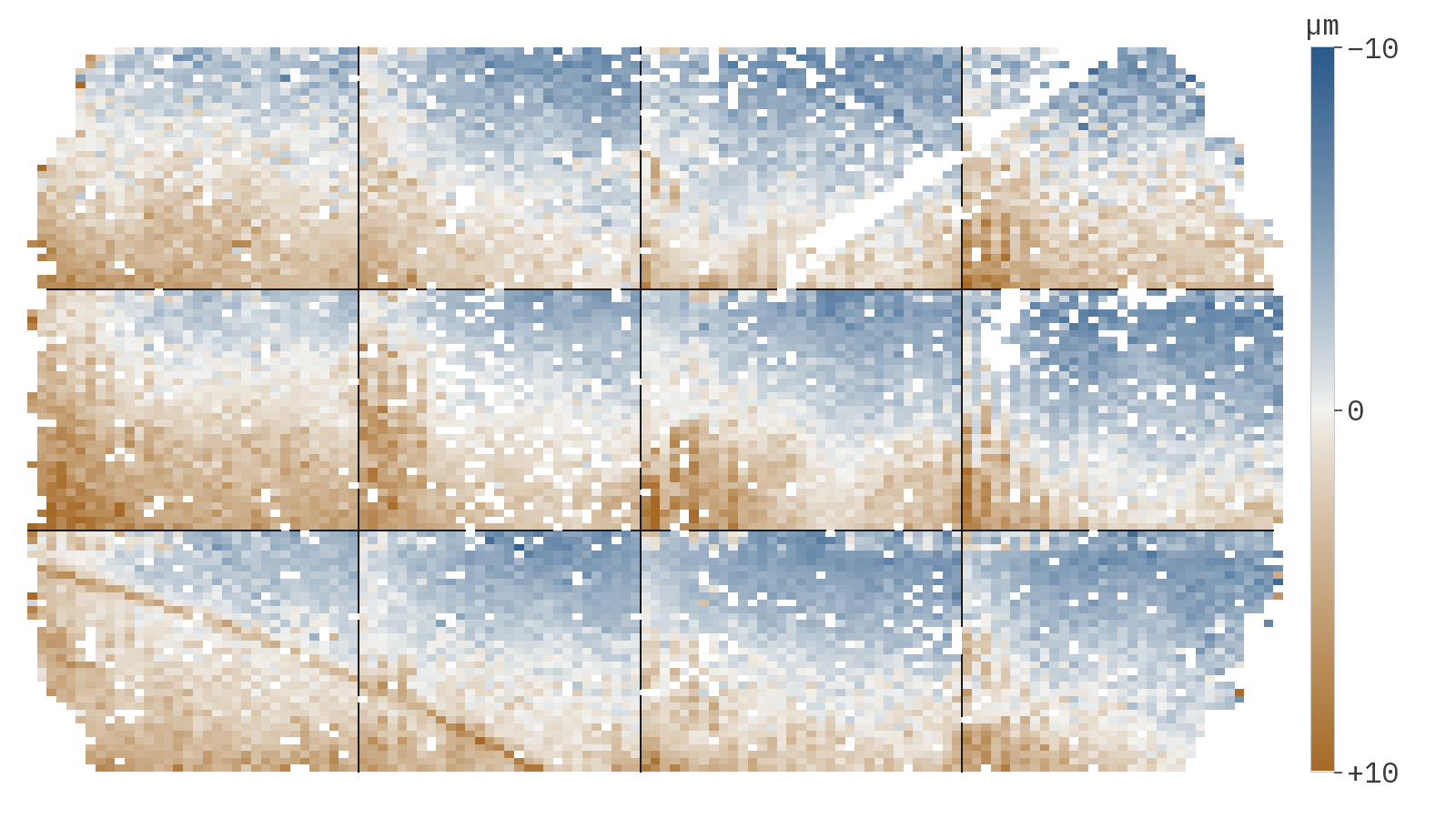
This finding led to a redesign of the wafer alignment. The resulting M.A.P. method replaces the sector-by-sector measurement with a calculation of the component positions from a small number of reference positions and has been used in series production since 2025.
What does this project show?
The project shows the analytical side of taking over and modernising existing software: a production problem that is initially hard to reproduce is traced back to a measurable technical cause using additional data, purpose-built analysis tools and statistical evaluation.
The root cause analysis did not stop at the diagnosis. The proven error pattern led to the follow-up contract for a new alignment of the wafer inspection systems.
The complete path from the takeover of the existing machine software through the root cause analysis and the development of the new alignment to its use on 134 systems is described in the case study Machine software for 134 wafer inspection systems taken over.
Key facts
- Service
- Takeover and modernisation
- Industry
- Semiconductor manufacturing
- Period
- October 2023 to February 2024
- Technology
- Log parser, WebGL, three.js, statistics, MVTec HALCON.