
Wafer alignment for inspection systems: 84% faster with 4 to 5 µm accuracy
EPSIA developed a new wafer alignment for a semiconductor manufacturer's wafer inspection systems and integrated it into the existing machine software.
The M.A.P. method (Map Alignment and Positioning) calculates the positions of the components from a small number of optically determined reference positions, instead of measuring the entire wafer sector by sector before production starts.
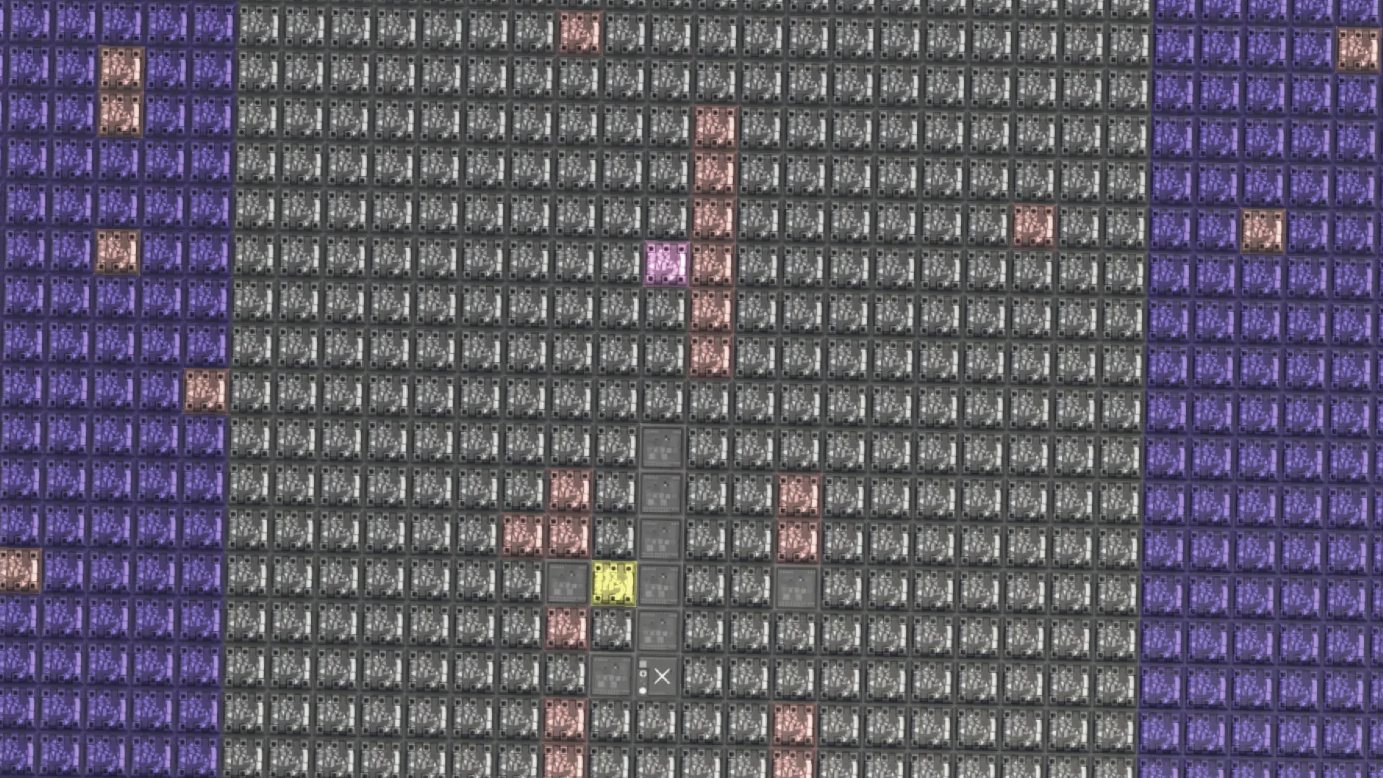
Starting point
The wafer inspection systems contact every single component with probes. To do this, the control software must know the position of the components on the wafer with high accuracy.
The previous method measures the wafer sector by sector with a camera before production starts. An earlier root cause analysis by EPSIA had revealed a systematic problem: at the edge of the camera's field of view, position errors of 5 to 10 µm occurred. At the same time, the complete pre-measurement took several minutes for every wafer.
Solution
With M.A.P., EPSIA developed a new method that calculates the positions of the components from the existing wafer map and a small number of optically determined reference positions.
- The system locates selected reference positions with the camera using a newly developed HALCON procedure.
- From the measured positions, the software determines the offset, rotation and scaling of the wafer.
- From these, the position of every single component on the wafer is calculated.
- The existing axis correction matrix from the stage calibration and a hardware-related rotation angle are included in the calculation.
- Plausibility checks detect special cases; if necessary, the system can fall back on the previous alignment method.
EPSIA developed and integrated the method without having its own production system. The software was first tested on a reference system at the machine builder in Berlin and then remotely in the customer's production in Asia.
Result
- Alignment of an 8-inch wafer was reduced from 7:44 to 1:16 minutes, around 84% less time.
- The actual pre-measurement was reduced from 6:12 minutes to 16 seconds.
- Positioning accuracy (3σ) is 4.2 × 2.6 µm with around 70,000 components and 5.1 × 1.6 µm with around 130,000 components per wafer.
- M.A.P. has been used in the customer's series production in Asia since summer 2025.
What does this project show?
The project shows how EPSIA develops existing machine software further in a targeted way when changes have to be integrated directly into a running production process.
The new alignment was developed without a production system of EPSIA's own, tested on a reference system in Berlin and remotely in Asia, and then transferred to series production. Its effect can be quantified both by the alignment time and by measured positioning accuracy.
The complete path from the takeover of the existing machine software through the root cause analysis to the new alignment and its use on 134 systems is described in the case study Machine software for 134 wafer inspection systems taken over.
Key facts
- Service
- Hardware-related systems
- Industry
- Semiconductor manufacturing
- Period
- since 2024, ongoing
- Technology
- C++, Qt, MVTec HALCON, MinGW, qmake, CAN, EtherCAT, MySQL, Unity.